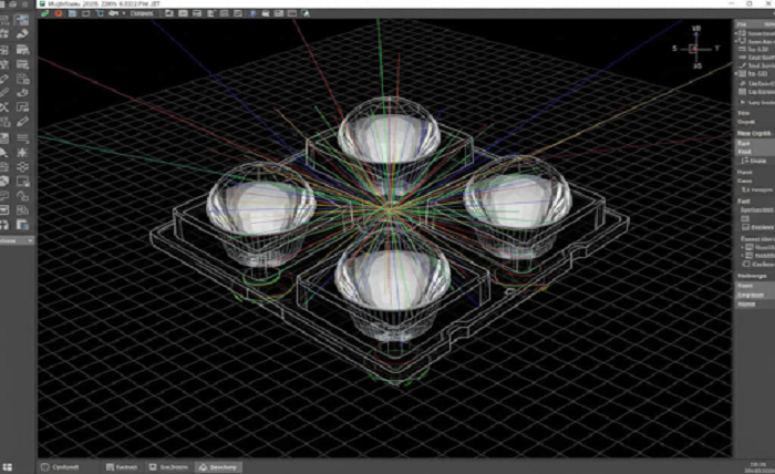
In the modern lighting industry, the barrier to entry for optical engineering has seemingly lowered. With powerful ray-tracing software becoming more accessible, it is easy to assume that anyone with a license can design a high-performance lens. On a computer screen, everything looks perfect: the beam angle is exact, the efficiency is 100%, and the light distribution is flawless.
However, a stunning simulation does not guarantee a successful product. In fact, “perfect” simulations are often the primary cause of failure in mass production.
For lighting manufacturers and industrial designers, understanding the chasm between digital theory and physical reality is crucial. Successful LED optics design is not just about manipulating photons in a virtual void; it is about engineering a component that can survive the chaotic, imperfect world of manufacturing constraints.
The Trap of Ideal Conditions
The fundamental flaw in many junior optical designs is the assumption of “Nominal Zero.” In simulation software, the LED chip is treated as a perfect point source located at coordinates (0,0,0). The lens is assumed to be perfectly clear, and its geometry is mathematically absolute.
But in the real world, “Nominal Zero” does not exist.
LED Placement: The pick-and-place machine mounting the LED onto the PCB has a tolerance (e.g., ±0.1mm).
Floating Height: The thickness of the solder paste varies, changing the focal distance between the die and the lens.
Chip Variations: Even within the same binning, the light emitting surface (LES) of an LED can have slight brightness variations.
If an optical design is too aggressive—relying on razor-thin tolerances to achieve a specific beam angle—these minor real-world shifts will ruin the performance. A spotlight designed for 10° might output 15° with a distorted halo simply because the LED was soldered 0.05mm off-center.
Design for Manufacturability (DFM): The Hidden Art
This is where the true expertise of optical design comes into play. Experienced engineers do not design for the “best case” scenario; they design for the “worst case.”
This process is known as Tolerance Sensitivity Analysis. By running Monte Carlo simulations, engineers can predict how the lens will perform if the LED shifts, rotates, or tilts. A robust design might use texturing techniques (like Micro-lens arrays or frosting) on the lens surface. These features act as optical buffers, smoothing out the artifacts caused by assembly errors. While this might reduce the theoretical efficiency by 1-2%, it ensures that 99.9% of the mass-produced fixtures pass quality control.
Material Physics: Beyond Refractive Index
Another critical oversight in pure software design is the behavior of materials. A simulation defines the material simply by its refractive index (e.g., 1.586 for Polycarbonate). However, physical materials are dynamic.
Asahi optical lenses are engineered with a deep understanding of thermal dynamics. When a high-power LED fixture heats up, two things happen:
Thermal Expansion: The lens physically expands. If the design does not account for this growth, the lens can push against the holder or the PCB, causing stress warping or even cracking.
Refractive Shift: The refractive index of polymers changes slightly with temperature (dn/dT).
An optic that works perfectly in a 25°C lab might fail in a 60°C operating environment. Professional LED optics design involves choosing the right material—whether it be PMMA, PC, or Silicone—matched to the specific thermal load of the application.

From Prototype to Steel: The Tooling Reality
Once the design is finalized, the transition to tooling (mold making) is the final hurdle. A lens surface defined by a complex polynomial equation must be cut into steel using diamond-turning machines.
Here, the concept of “Draft Angle” becomes vital. If a designer creates a lens with vertical walls (0° draft), it cannot be ejected from the mold without scratching. The optical engineer must work in tandem with the mold engineer to ensure that the optical surfaces are ejectable while maintaining the required light distribution.
This is why integrated manufacturers often outperform design-only firms. Companies that handle both the optical design and the injection molding understand the limits of the machinery. They know how to optimize the “gate” location (where the plastic enters the mold) so that the injection scar does not interfere with the main light beam.
Conclusion: Partnering for Precision
In the race to launch new lighting products, it is tempting to rely on quick, automated simulations. But light is unforgiving. A shadow in the wrong place or a glare spike can result in a failed project or a product recall.
The value of a partner like Asahi Optics lies in the ability to bridge the gap between the digital and the physical. By combining advanced ray-tracing capabilities with decades of molding and material experience, manufacturers can deliver lenses that don’t just work on a computer screen—they perform flawlessly in the real world.